RISC-V Hardware Design: Debug via BSCAN Chain - Edgeboard RISC-V Series
Created on
27/02/20 13:00
Modified on
27/02/20 15:40
Filed under
RISC-V
Tags
risc-v debugging fpga embedded
Intro
This article is a part of the Edgeboard RISC-V series. Check out other articles as well if you came in through a search engine.
After setting up the hardware system, we need a way to test if the system is actually running. The BootROM is the location where the reset vector points to, but to change the code in the BootROM one needs to resynthesize and reimplement the design, which can take up to an hour for a Zynq UltraScale+ device on the development system. As a result, a fast, external debug method is needed, and GDB with OpenOCD satisfies this requirement perfectly. This article covers how the BSCAN tunnel mechanism was adapted to work on Zynq UltraScale+ devices.
BSCANE2 primitive on Xilinx devices
While it is possible to use PL GPIO and connect a separate JTAG cable to directly access the Rocket Chip JTAG TAP, but I failed to plan ahead and had just purchased one JTAG cable, and it's too much labour to switch between the cabling of Xilinx JTAG and that of the GPIO JTAG every time I want to program a bitstream or debug RISC-V. Fortunately, we can find that 7 Series and UltraScale architectures provide a BSCANE2 primitive:
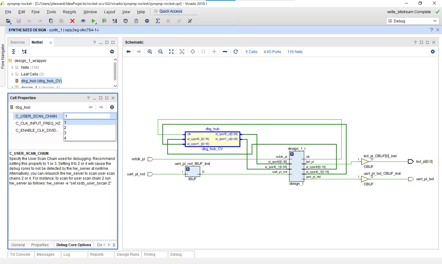
This design element allows access to and from internal logic by the JTAG Boundary Scan logic controller. This allows for communication between the internal running design and the dedicated JTAG pins of the device. Each instance of this design element will handle one JTAG USER instruction (USER1 through USER4) as set with the JTAG_CHAIN attribute. To handle all four USER instructions, instantiate four of these elements and set the JTAG_CHAIN attribute appropriately. For specific information on boundary scan for an architecture, see the Configuration User Guide for the specific device.
This indicates that we can send JTAG commands to a PL design through the user registers accessible on the PL TAP from the dedicated JTAG port of the ZynqMP chip. The user chains, specifically USER1 by default, powers the on-board debug facilities such as ILA, JTAG Master, or VIO:
Referring to UG470 7 Series FPGAs Configuration User Guide we can find out details about advanced features of JTAG on these devices besides user chains, for example programming a bitstream with OpenOCD from macOS.
There has already been a mechanism that utilizes the USER4 chain to tunnel requests to the RISC-V TAP: the BSCAN tunnel translator in Chisel and the BSCAN tunnel implementation in RISC-V OpenOCD. The solution will not work directly here however:
- The Zynq UltraScale+ platform uses a different JTAG IR for
USERxchains:0x20-0x23for 7-series FPGA0x920-0x923for Zynq UltraScale+- This can be confirmed in the BSDL Models released by Xilinx
- Addressed in OpenOCD via commit
- The Zynq UltraScale+ TAP scan chain structure is different from normal FPGAs
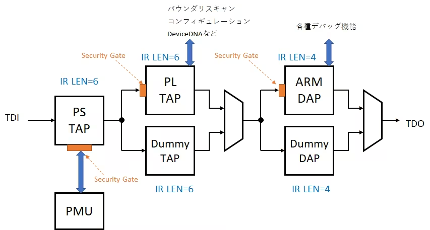
- The user chains are located on the PL TAP (IR LEN=6) which is on the chain concatenated with the PS TAP (IR LEN=6), resulting in a single TAP with IR LEN=12
- There is an ARM DAP sitting between the combined PS/PL TAP and TDO, which shifts the input and output data (DR contents) by one bit (bypass), addressed in the following commits:
A picture from the article 「ZYNQ UltraScale+ MPSoCのJTAGのしくみ」, which explains the JTAG structure of Zynq UltraScale+ in detail:
GDB
After understanding the user chain mechanisms for Zynq UltraScale+, we can finally attach GDB to our RISC-V core. An OpenOCD config originally for debugging the APUs (Cortex-A53) on ZynqMP was adapted to enable RISC-V debugging. Stop hardware server (to avoid libusb conflict with OpenOCD), launch OpenOCD, and attach gdb:
(the hwserver)
# systemctl stop hwserver
# openocd -f openocd.cfg -c "init_riscv"
(the development machine)
# riscv64-linux-gnu-gdb
...
(gdb) target remote 192.168.79.129:3333
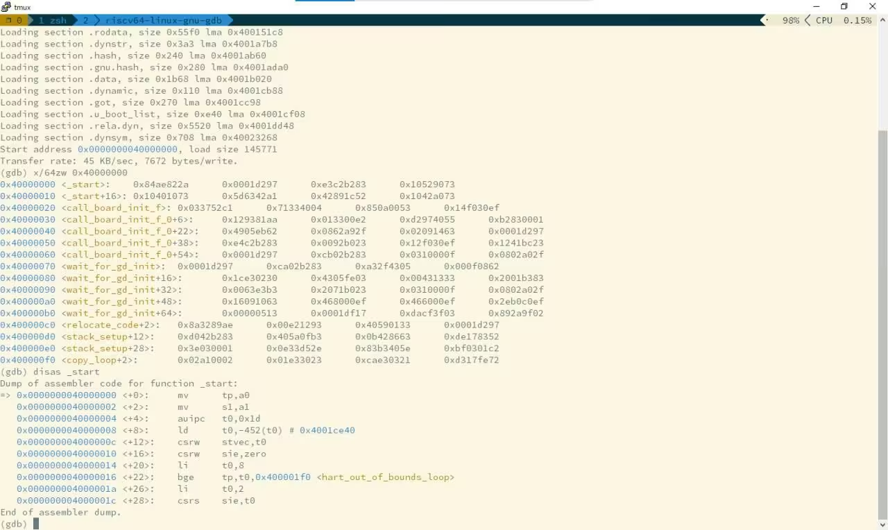
The following picture shows loading an OpenSBI ELF (which will be covered in the follow-up software articles) to DDR at 0x40000000:


