RISC-V Hardware Design: System & Block Design - Edgeboard RISC-V Series
Created on
25/02/20 14:40
Modified on
27/02/20 15:40
Filed under
RISC-V
Tags
risc-v fpga zynq embedded
Intro
This article is a part of the Edgeboard RISC-V series. Check out other articles as well if you came in through a search engine.
After setting up the development environment and testing the board, we can finally start designing the RISC-V hardware system. This part of the series describes the configuration of the Rocket Chip SoC generator, which is used to generate the processor IP used in this project, as well as the "uncore" peripheral setup. The hardware setup are published in the rocket-zynqmp repository. A follow-up article, also about hardware platform design, will focus on enabling GDB debugging for the RISC-V core.
Configuring Rocket Chip
Rocket Chip is an SoC generator, which is necessary for instantiating the Rocket Chip CPU core and using it. The CPU core and uncore components are implemented with the Chisel/FIRRTL HDL, while the SoC generator, Diplomacy, which is used to automatically negotiate various bus structures between components in the SoC, is written in Scala. Thanks to the flexibility of Chisel generators as well as the Scala language, the Rocket Chip can be configured to adapt to different needs quite easily.
The exact config I have been using on the Edgeboard can be found here. Listing the main differences from DefaultConfig:
- Main memory (DRAM) has been relocated to
0x40000000, with a size of0x3ff00000.- The Edgeboard has 2GB of DDR4 RAM available. Under this configuration, the APU in Zynq PS can use
0x00000000, size0x40000000(1GB) as main memory, and the higher ~1GB can be used by RISC-V.- The highest 16MB of RAM is reserved by the PMU in ZynqMP.
- The Edgeboard has 2GB of DDR4 RAM available. Under this configuration, the APU in Zynq PS can use
- MMIO has been relocated to
0xe0000000.- According to UG1085, most of the PS peripherals are mapped in
0xe0000000to0xffffffff. In order to use PS peripherals in RISC-V, specifically GEM and MMC, we have to follow this arrangement as well.
- According to UG1085, most of the PS peripherals are mapped in
- There are 4 interrupts to the interrupt controller, listed in the order of IRQ:
- UART
- Ethernet (Zynq GEM)
- Ethernet Wake
- MMC
- The system runs at 100MHz.
- This is used for a correct
timebase-frequencyas well as other frequency specifications in the generated device tree.- Although the generated device tree is not used after all...
- This is used for a correct
- 8 hardware breakpoints, instead of the default of 2, are instantiated.
- 2 of them are just not enough for any proper debugging with GDB later on.
- You may have heard of software breakpoints, but they don't work well in the situation we're in. The follow-up article about debugging will cover this.
- 1 big core (RV64GC) is instantiated.
- Unlike the ZCU102 with ZU7EG which can house 4 big cores with barely over 50% LUT use, the Edgeboard uses ZU3EG and will house 1 big core with about 55% LUT use.
- The reset vector has been changed to
0x10000.- The original setup has it at
0x10040, which is just a bootloop application. This change enables meaningful code to be run on the processor.
- The original setup has it at
Besides configuration, a top module implementation and optional wrapper are needed for actual instantiation of the SoC. We will not go through how the various traits contribute to the final generation of the SoC, or how Diplomacy works. After running the generator and FIRRTL compiler, we get our generated Verilog file, which contains the RocketTop module ready for simulation or synthesis.
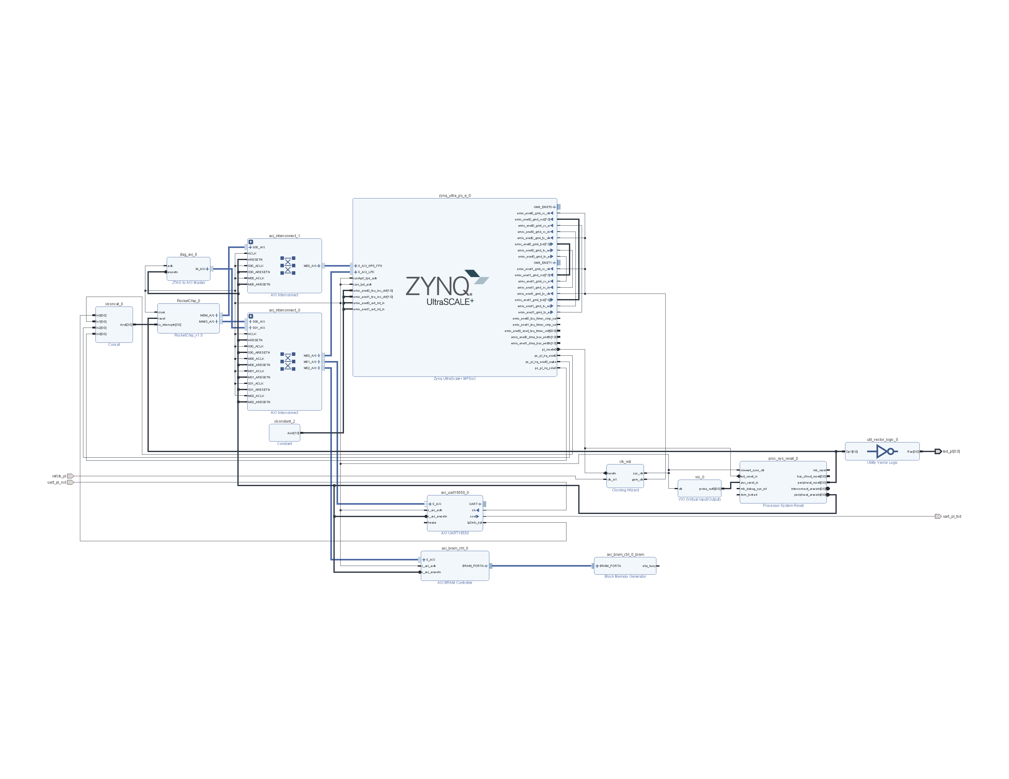
Xilinx IP Block Design
The Rocket Chip SoC instantiated in this project communicates with the external world over AXI4 MM interfaces, and is instantiated in Vivado in a Block Design or, officially, the Vivado IP Integrator. This is the usual flow for a complex system design, especially one with some kind of CPU, on a Xilinx device with the Vivado suite. Despite that it's possible to eliminate MMIO entirely and use all peripherals from SiFive (as done by @Sequencer here), we still adopt the IP Integrator flow.
To save time that would be wasted if every time Rocket Chip needed re-synthesizing despite only small changes to the BootROM, AXI topology, or debug cores, we package the Rocket Chip module as a separate IP such that the synthesis results can be cached. Other IP modules used in the project are:
- Zynq UltraScale+ MPSoC (the PS block)
- DRAM access, peripheral access
- System reset
- The PS fabric clock output was deliberately avoided due to its unpredictable behavior (which caused a lot of confusions together with @jiegec)
- AXI UART16550
- For serial access
- The board lacked a proper board file, so it's required to only make UART
sinandsoutexternal, or unconstrainted ports that does not actually exist on board will prevent bitstream generation
- The board lacked a proper board file, so it's required to only make UART
- For serial access
- AXI BRAM Controller and Block Memory Generator
- Used together for hosting the Secondary BootLoader - OpenSBI with U-Boot as payload. This will be explained in detail in the follow-up RISC-V software system articles.
- Various utility IPs
- AXI Interconnect for data width, protocol conversion and xbar feature
- JTAG to AXI master for debugging memory and device access
- VIO (Virtual Input/Output) for RISC-V reset signal (Edgeboard does not have any push buttons wired to PL)
- Processor System Reset, Clocking Wizard for clock and reset generation
- Utility Vector Logic, Concat, Constant for manipulating basic signals
The complete block design is as shown below. Download PDF if you want to examine the details. Also check out the TCL script for recreating the block design in Vivado.
With all the setup done, we can now launch the implementation run in Vivado, generate a bitstream, and get ready for on board tests with GDB through JTAG.
Footnote: a PS DDR complication
During the development process, I've spent a lot of time trying to debug weird problems with DDR access from RISC-V. Sometimes the DRAM appears to be working and will host C stacks for some time, but then the stack gets corrupted mysteriously. Loading code into DDR won't work at all: the content is different from what had been loaded when trying to read back.
The debug process went rather extensive, involving trying to memtest from PS and PL, with RISC-V or without RISC-V (with JTAG to AXI master), over different interconnect ports PS has to offer. Finally, in an orchestrated debug attempt involving both PL and PS, the following pattern was identified:
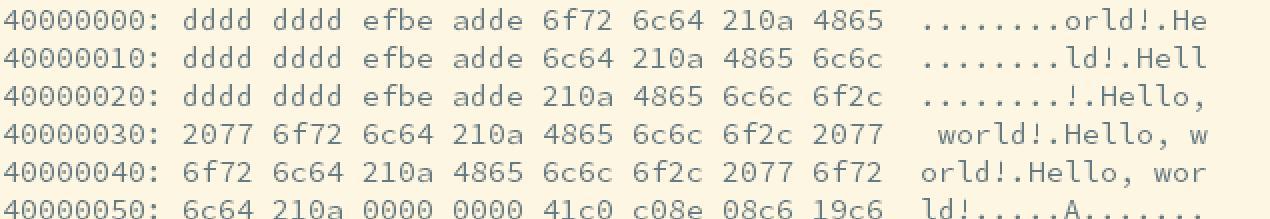
The pattern was that PS wrote continuous Hello, world! pattern to DRAM assigned for RISC-V, and RISC-V writing simple memtest incremental patterns word-by-word. Obviously this is a data width problem. After changing the AXI slave data width from 64 to 128, everything worked like a charm.
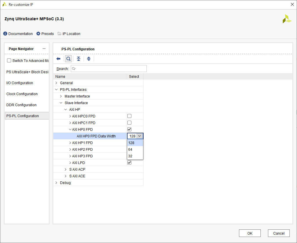
This behavior is counter-intuitive and nowhere to be seen in the Technical Reference Manual. I would appreciate it greatly if someone familiar with the ZynqMP can explain to me why this happened. If you have any clues, please don't hesitate to contact me.